(+49) 0381 7006080
Development Process - Step 2
PCB Layouts Placing and decoupling

Increasing complexity, ever faster signal speeds, miniaturization and the variety of PCB technologies available place increasing demands on the development of PCB layout for assemblies. Based on a printed circuit board manual, pironex electronics developers create production data for the printed circuit boards. Benefit from our many years of experience in designing PCB layouts for single- and multi-layer PCBs. The unbundling of memory and processor assemblies is impedance-controlled and manual.
The manufacturability and testing capability of the assemblies is coordinated with the EMS service providers for the future assemblies.
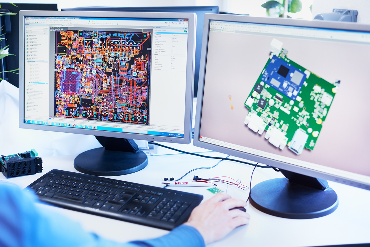
PCB Layouts
pironex GmbH implements customer-specific printed circuit board layouts. In the first step, the hardware developers adapt the contours of the circuit board. This is done in close coordination with the housing designers. The components and connectors are then placed on the circuit board. In this work step, there is close cooperation with the housing design as well. After placement, the electrical connections are routed using the modern layout tool Altium Designer. Complex circuit board constructions usually have to be unwired manually.
It is always important that the assemblies are manufactured inexpensively. This means that the printed circuit boards must be aligned with the relevant machine guidelines and design guidelines.
Working Steps for PCB Layout of Circuit Boards
- Examination of the existing concept
- Creation of required libraries for the passive and active components
- Adaptation of the electronic circuit components including VHDL components
- Integration of FPGA and CPLD functional assemblies
- Analogue or digital simulation of the electronic circuit
- Implementation of the mechanical CAD specification
- Impedance calculation of the circuit and PCBs
- Unbundling (routing) of the multi-layer circuit board
- Detailed documentation
- Archiving of libraries (components, footprints)
- EMC compliant layout as Altium Designer PCB File
- Creation of production documentation (Gerber data, drilling data, assembly data)
Libraries
The development department uses carefully parameterised and maintained libraries so that the information used on the electronic components is up to date. This ensures traceability to the basic component data and discontinued components can be replaced at any time.
Especially during times of component shortages and poor availability of passive and active components, the direct comparison of the distribution databases is crucial for the successful course of the project.
Altium Designer
The electronics development department uses Altium Designer, a schematic and PCB design tool, to develop schematics. The printed circuit boards (PCB) are routed with Altium's layout tool. With the tool, all special cases such as delay-time-controlled routing, differential-pair and impedance-controlled routing, for example for high-speed designs, can be implemented professionally.
After completion of the customer-specific circuit board design, the work results are handed over to the customer in the form of layout and production data for any further processing and production.
We are listed as Qualified Service Partners of Altium Designer.